6 Layer PCB Board-Stackup, Thickness, Fabrication, and Price

Contents

6 layer PCB boards have three dielectric layers and three conductive layers. The dielectric layers typically consist of fiberglass or another insulating material, while the conductor layers are copper.

PCB 6 Layer Stack up

What is 6 Layer PCB Board?

The 6-layer PCB is the same as the 4-layer PCB board we have introduced, and it belongs to a kind of multilayer printed circuit board.  A 6-layer PCB Board can be regarded as a standard four-layer circuit board plus two additional signal layers. Therefore, a standard 1.6mm 6-layer PCB board stackup is Top Layer and Bottom Layer, 3 Prepreg Layers, 2 internal routing layers, 1 internal Ground layer, 1 internal power layer, 2 Core layers. This stacking method can be Improve the EMI effect to a large extent.

6 Layer PCB Board

6 Layer PCB Stackup Applications

6-layer PCB and even multi-layer PCB are widely used in various industries due to their more wiring capabilities and superior performance.

  • Consumer electronics: 6-layer PCB stackup is chosen by most high-end consumer electronics products, including microwave ovens, smartphones, wearable devices, etc.
  • Telecommunications: such as GPS, satellites, signal transmission, and telecommunications base stations.
  • Medical devices: Medical devices such as scanning equipment, X-ray machines, and heart monitors use 6-layer PCBs.
  • Industrial control: 6-layer PCB stacking is suitable for most industrial equipment, because it has the durability and stability required for industrial production, and can adapt to different production environments.

6 Layer PCB Stackup

Standard and Typical 6 Layer PCB Stackup

PCB stack-up refers to the copper layer, core board, and PP layer constituting the PCB board. The laminated structure of PCB boards with the same number of layers can meet different user requirements. We need to know that multilayer PCBs, such as 6-layer PCBs, have at least three conductive layers, and each layer is electrically connected through holes.

The benefits of PCB stacking

Multilayer circuit boards can create more complex and space-saving printed circuit boards. PCB stacking has other advantages:

  • Maximize the function of circuit board: multilayer circuit board can significantly improve the signal transmission speed and function of electronic equipment so that the circuit board has more powerful functions;
  • Improve durability: Multilayer PCB stacking can protect the inner layer of the circuit board from external factors and enhance durability;
  • Effectively reduce radiation: the perfect PCB stacking design can minimize equipment radiation, especially in the laminated design of high-frequency and high-speed circuit boards. In addition, if the impedance design is unreasonable, it is easy to cause more significant EMI radiation than ordinary PCB;
  • Effectively reduce manufacturing cost: excellent multilayer PCB stacking design can also achieve lower manufacturing cost by placing multiple circuits on the same circuit board
  • Effectively reduce signal crosstalk: good PCB stack-up can mitigate the problems of poor impedance and signal crosstalk.
standard 1.6mm 6 Layer PCB Stackup and Thickness

Fig.1
standard 1.6mm 6 Layer PCB Stackup and Thickness

Although the 6-layer PCB stack mentioned above is standard, the standard is not the best. The following is a comparison of three other 6-layer PCB stacking methods.

What is the best 6 Layer PCB Stackup?

The following is a set of typical 6-layer PCB circuit board stacks for reference.

6 Layer PCB Stackup

Fig.2 6 Layer PCB Board Stackup

The structure is:

  1. Signal Layer
  2. Ground plane
  3. Signal Layer
  4. Power Plane
  5. Ground Plane
  6. Signal Layer

This may not be your most satisfactory 6-layer PCB stack structure because the signal layer in the circuit board does not have any shielding, and two of the signal layers are not adjacent to any ground plane. As signal integrity and performance become more and more important, such a 6-layer PCB stack structure has been gradually abandoned.

6 Layer PCB Stackup from PCBELEC

Fig.3 6 Layer PCB Stackup from PCBELEC.COM

In this 6 layer PCB stack-up is the signal layers are reduced to 3 to add a ground layer:

  1. Top Signal Layer
  2. GND1
  3. Inner Signal Layer
  4. Power Plane
  5. GND2
  6. Bottom Signal Layer

This 6-layer PCB stack-up places each signal layer close to the ground plane to obtain the best return path characteristics. In addition, putting the power and ground planes adjacent to each other creates planner capacitance. But the same disadvantage is that you will indeed lose a signal layer for routing.

6 Layer PCB Stackup and Thickness

Fig.4

6 Layer PCB Stackup and Thickness

3 Types of 6 Layer PCB Stackup

Fig.5

3 Types of 6 Layer PCB Stackup, the right one is best.

1.0mm 6 layer PCB Stackup

Fig.6

1.0mm +/-0.1mm finished 6 Layer PCB Stackup

63 mil 2.0mm thickness 1.6mm 6 Layer PCB Stackup

Fig.8

63 mil 2.0mm thickness 1.6mm 6 Layer PCB Stackup

6 Layer PCB Design

6 Layer PCB Design Tutorial and Design Software

Creating a suitable stack structure will have a massive impact on the design of the 6-layer circuit board. Fortunately, at present, PCB design software is becoming more and more powerful, and you can thoroughly complete the laminated design you need in the PCB design software.

How to choose a PCB design software that suits you? We have listed here 30 free PCB design software for you to download.

On the right is a video tutorial of a 6-layer PCB design using OrCAD; I hope it will be helpful to you.

Learn more about 4 Solutions to Reduce EMC in 6-layer PCB Design

6 Layer PCB Fabrication

Quick Turn 6 Layer PCB Board Manufacturing

Compared with double-sided circuit boards and 4-layer circuit boards, 6-layer circuit boards have more layers and are therefore more conducive to routing. However, at the same time, the fabrication cost and production difficulty of 6-layer circuit boards are also Will increase.

A 6-layer PCB board is built by laminating PCB layers on the PCB core. Once the circuit is etched on the PCB core and the third and fourth layers are done, the second and fifth layers are laminated under high temperatures and pressures. Then the circuit is etched on the second and fifth layers. And the top and bottom layers are also laminated on the 4-layer board, and the circuit is etched. And the solder mask is spayed on the top and bottom layers, and the surface finish is processed on the PCB pads.

There are two circuit etching methods for the PCB layer, they are:

  • Positive plane etching
  • Negative plane etching

With the continuous development of SMT (Surface Mount Technology) and the continuous introduction of a new generation of SMD (Surface Mount Devices), such as QFP, QFN, CSP, BGA (especially MBGA), electronic products are more intelligent and miniaturized, so Promoted major reforms and advances in PCB industrial technology.

Therefore, the advancement of PCB manufacturing technology has also made the manufacturing of 6-layer PCBs easier.

6 Layer PCB Fabrication - Drilling

Fig.9

6 Layer PCB Fabrication – Drilling

Materials for 6-layer PCB manufacturing

The printed circuit board must be flame-resistant, not burn at a specific temperature, but can only be softened. The temperature at this time is called the glass transition temperature (Tg point), and this value is related to the dimensional stability of the PCB board.

The ordinary PCB material with a Tg value is more than 130 degrees, the high Tg value is generally greater than 170 degrees, and the medium Tg value is approximately 150 degrees.

Usually, printed circuit boards with Tg ≥ 170°C are called high Tg PCB.

Multilayer circuit boards, such as 6-layer PCBs, generally use high TG value plates during manufacturing.

Normal TG material with TG130-135High TG material with over TG170

Manufacturer/Brand

Material

Manufacturer/Brand

Material

ShengYi

S1141ShengYiS1000-2
S1155S1141

NanYa

NP-140TLS1170

KingBoard

KB-6160S1165
  ISOLAFR406/FR408
  ARLONHigh Tg210 11N
  GETEKHigh Tg180 ML200/RG200
  NELCOHigh Tg175 N4000-6/N4000-11
  High Tg190 N4000-12
  High Tg210 N4000-13
  ITEQIT180
High-frequency material (RF boards)Prepreg Material Information

Manufacturer/Brand

Material

Manufacturer/Brand

Material

RogersRO4000 SeriesKingBoardKB-6050 PrePreg
RT5000/RT6000 Series KB-606X
TacanicTLX Series  
Orcer RF-35/RF-60 Series  
High-frequency material (RF boards)
Prepreg TypeThickness (mm)Resin ContentDielectric Constant
21160.1255%4.5

7630

0.255%4.7
76280.18543%4.7
10800.07565%4.2

6 Layer PCB Manufacturer

How to choose the best 6-Layer PCB manufacturer?

Choosing a capable 6-layer PCB manufacturer is very important to realize your PCB design concept. A good multilayer PCB manufacturer must be efficient and reliable. Here are the factors to consider when choosing a 6-layer PCB manufacturer:

  • Rich experience: PCB manufacturing experience determines whether the manufacturer can successfully complete your 6-layer PCB manufacturing task. Therefore, it is crucial to choose a reliable manufacturer with long-term experience in 6-layer PCB manufacturing.
  • Certification and licensing: The best 6-layer PCB manufacturers must have qualified qualification certification, and the circuit boards produced by the best PCB manufacturers will meet the IPC standards of the PCB industry.
  • Quick Turnaround Time: Turnaround time is the time it takes to complete an order. You definitely want your manufacturer to be able to deliver high quality boards within a certain turnaround time. Also, your manufacturer should deliver good quality boards with good turnaround times.
  • Technical support: There are strong PCB manufacturers who can help you with your PCB design, and can provide you with technical support such as DFM, DFT, and DFA.
  • Customer Service: You definitely want your PCB manufacturer to meet your needs. You need to choose a PCB manufacturer that can respond to customer needs and complaints.

JHY is a reliable and trustworthy PCB manufacturer and supplier located in China, we were established in 2011, specializing in single-sided, double-sided and multi-layer rigid PCB, flexible PCB, rigid-flex PCB, HDI PCB, etc. Prototype PCB and high-volume PCB manufacturing services. We can fabricate and assemble cash PCBs from 1-64 layers.

6 Layer PCB Cost

6 Layer PCB prototype Price

JHYPCB is a professional multilayer PCB manufacturer in China with a good price. We provide customers with low-cost, high-quality, and fast-turnover 6-layer PCB prototype production services.

6-layer PCB prototype fabrication can quickly verify your stack up and design, find errors and defects in time and reduce losses before mass production.

5-7 days delivery for 6 layer PCB prototype, and 72 hours for express prototyping.

You can get a quick free quote for 6 layer PCB, simply by email send Gerber, quantity, etc. to sales@pcbjhy.com.

6 Layer PCB

6 Layer PCB FAQs

  1. The number of PCB layers is different: a 6-layer PCB has two more layers than a 4-layer PCB, making a 6-layer PCB more complicated than a 4-layer PCB.
  2. The stacking structure is different: there are two additional signal layers between the planes of the 6-layer PCB stack, which also increases the procurement cost of the 6-layer PCB stack.
  3. The impedance characteristics are different: If we compare the 6-layer PCB stack with the 4-layer PCB stack, the impedance is lower.
  4. A 6-layer PCB stack-up has more space and therefore comes with less wire connection on each layer than a 4-layer PCB stack-up.
  5. 6 layer PCB stack-up works more efficiently and performs better than a 4-layer PCB stack-up.

Many factors affect the price of 6-layer PCB, which are summarized as follows:

  1. The larger the size of the 6-layer PCB, the higher the manufacturing cost;
  2. The price of a 6-layer PCB with unique production processes such as buried blind vias will be higher;
  3. 6-layer PCB materials, such as High Tg170 and High Tg180 boards, will be more expensive than ordinary FR4 boards;
  4. Quantity and quality of components: As the number of components increases, the assembly price of the 6-layer circuit board will also increase; if the quality of the components selected is better, the cost will be more.

  • Step 1. Editing the schematic diagram: After drawing the schematic diagram, don’t forget to check the error. And check the package manager to check the component package.
  • Step 2. Create a new PCB file, set the 6 layer PCB layer structure: After creating a new one, you can import the schematic netlist to a PCB file for 6-layer PCB manufacturing.
  •  Step 3. Layout: The main principle of layout in 6-layer PCB manufacturing is to partition well. Moreover, the partition of analog devices and digital devices,Which can reduce interference,Because the interference generated by digital signals is significant, and the anti-interference is also vital.
  • Step 4. Production of ground plane: 6-layer PCB manufacturing has two layers of ground: AGND and DGND. Generally, both are separated and located on the second and fourth layers, respectively. So the operation of the ground network is relatively easy. The ground network pins of the top and ground components are led out with wires and connected to the corresponding network through the via hole. Use as few pads as possible during the connection process because the pads will bring capacitance effects and increase interference.
  • Step 5. Production of power plane: Since the multilayer PCB board will not have only one working voltage value, the power layer should be divided.
  • Step 6. Routing: Make the power layer and ground layer well. And then, you can route the signal lines. When routing during 6-layer PCB manufacturing, the critical high-speed signal line is best to go to the inner signal layer.
  • Step 7. DRC inspection: This step is very important for 6-layer PCB manufacturing. After the PCB drawing is completed, it must be checked.

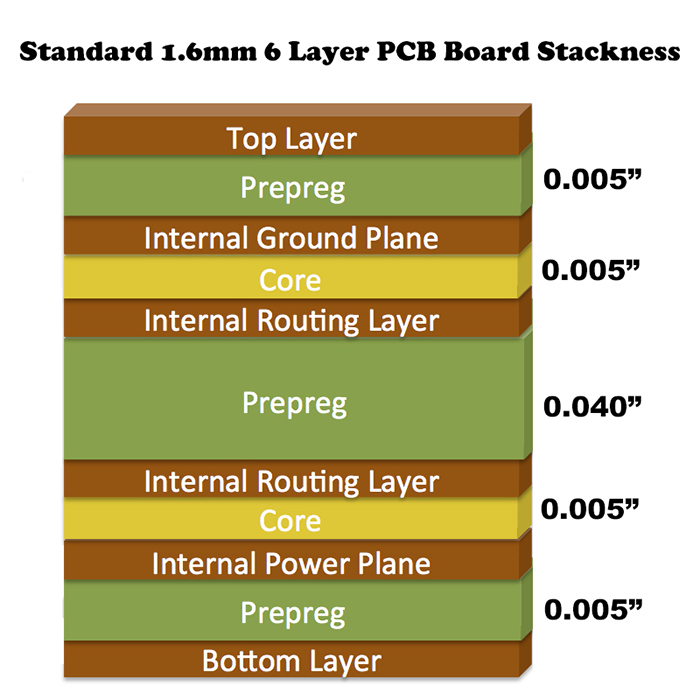
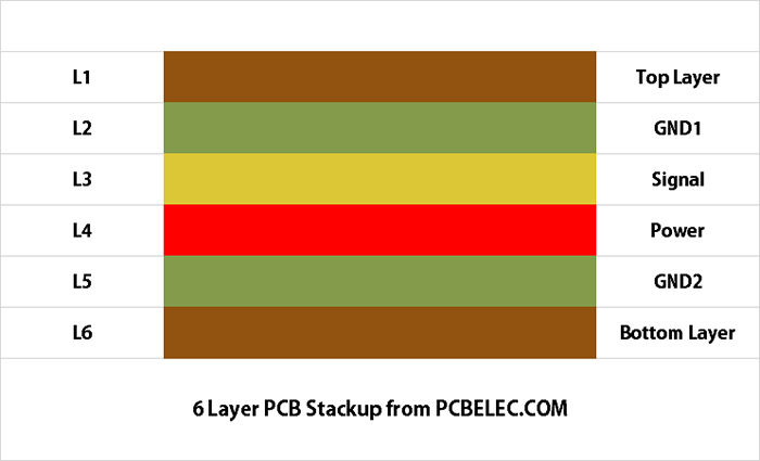
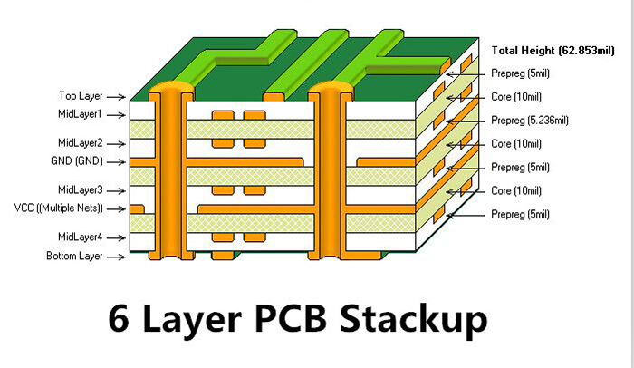
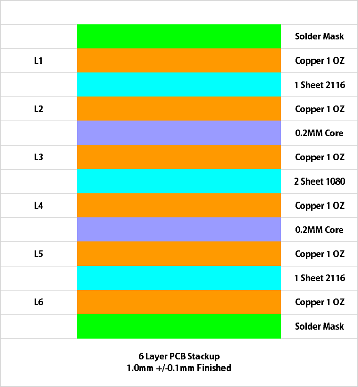
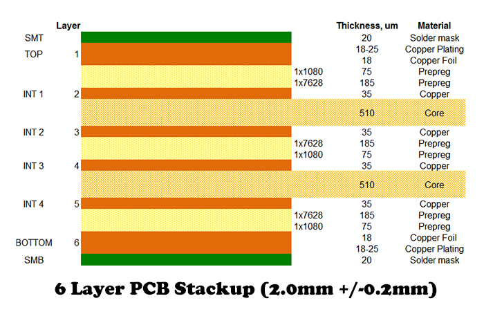
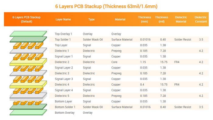
PCB Stack-up describes the construction of a multilayer circuit board in sequential order. It provides vital information like material thickness and copper weights required to manufacture a PCB. Stack-ups are also referred to as build-ups. The stack-up also gives the details of trace width for different controlled impedance traces such as 50ohms, 100ohms differential.

PCB stack-up is mainly composed of metal foil, prepreg, and copper-clad laminate (core).

  • Metal foil: copper is the most commonly used metal foil in PCB structures.
  • Prepreg: it is a kind of interleaved glass cloth impregnated in epoxy resin. The resin remains semi-cured.
  • Copper-clad laminate(CCL): one or more prepreg layers are bonded with the top and bottom copper foils to form a copper-clad laminate. CCL is also known as the core.
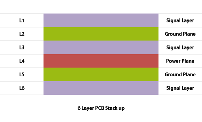
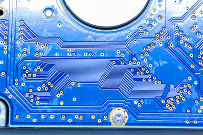
  • Power and ground layers in PCB stack-up: The power plane is a copper layer connected to the power supply. It is often designated as VCC in PCB design. The primary function of the power plane is to provide a steady voltage supply to the printed circuit board. In the multilayer PCBs, if a component needs to draw power, it is connected to the via that makes contact with the power plane. Similarly, the ground plane is a plane of flat copper connected to the common ground point in the PCB.

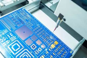
The PCB lamination is the process of placing the stack-up under high temperature and pressure to bond prepreg and copper foil to the base PCB inner layers. The temperature and pressure values are mentioned in the datasheets of the chosen PCB materials.

PCB Laminator

PCB Laminator

The thickness of the PCB board mainly depends on copper thickness, the material used, the number of layers, the operating environment, and other factors. The standard thickness of a conventional PCB is about 62 mils (1.57 mm). Nowadays, with the increase of the weight and number of copper layers in various applications, PCB becomes more complex. Therefore, PCBs tend to become thicker. According to the customer’s requirements, PCB manufacturers are now manufacturing two new standard thickness PCBs, 93 mils (2.36 mm) and 125 mils (3.17 mm) (150% and 200% of the old standard thickness).

With the progress of electronic technology, electronic equipment has become smaller and thinner. However, more and more electronic components and routing need to be used, so it has become more complex.

The single-layer circuit board has been unable to meet the growing complex needs. Therefore, it is necessary to increase the number of layers in the stack of circuit boards to solve this problem.

Increasing the number of layers on the printed circuit board has the following advantages:

  1. Multilayer circuit boards can adapt to the complex circuit design required by modern electronic equipment. For example, the circuit design of a 6-layer circuit board has much more significant advantages than that of a double-sided circuit board;
  2. Multilayer circuit board means that the circuit board is thicker, so it is more durable than a single-sided circuit board;
  3. The manufacture of Multilayer PCB is more precise, and its quality is higher than that of single and double-sided PCB;
  4. Multilayer circuit board simplifies the design of electronic equipment and further reduces the weight of electronic equipment.

Scroll to Top